A Guide to HDI PCB boards - What are they and what are they used for?

A Guide to HDI PCB boards - What are they and what are they used for?
A High-Density Interconnect (HDI) Printed Circuit Board (PCB) 🔗 is an advanced type of PCB with a significantly higher wiring density per unit area compared to traditional PCBs. This increased density is achieved through various miniaturization techniques, making it possible to pack more components and routing into a smaller board space. HDI PCBs 🔗 are essential for modern electronic devices that require small form factors, lightweight design, and high levels of functionality.
Key Characteristics and Vias
The key to an HDI PCB's complexity and density lies in its specialized interconnect features. These include microvias (tiny laser-drilled holes, usually less than $150 \mu$m in diameter), blind vias (connecting an outer layer to an inner layer but not extending through the entire board), and buried vias (connecting only internal layers). Traditional PCBs rely mainly on larger through-hole vias. The use of these smaller, non-through-hole vias, often combined with fine lines and spaces ($\le 100 \mu$m), significantly frees up board real estate for component placement and dense signal routing.
Manufacturing Process
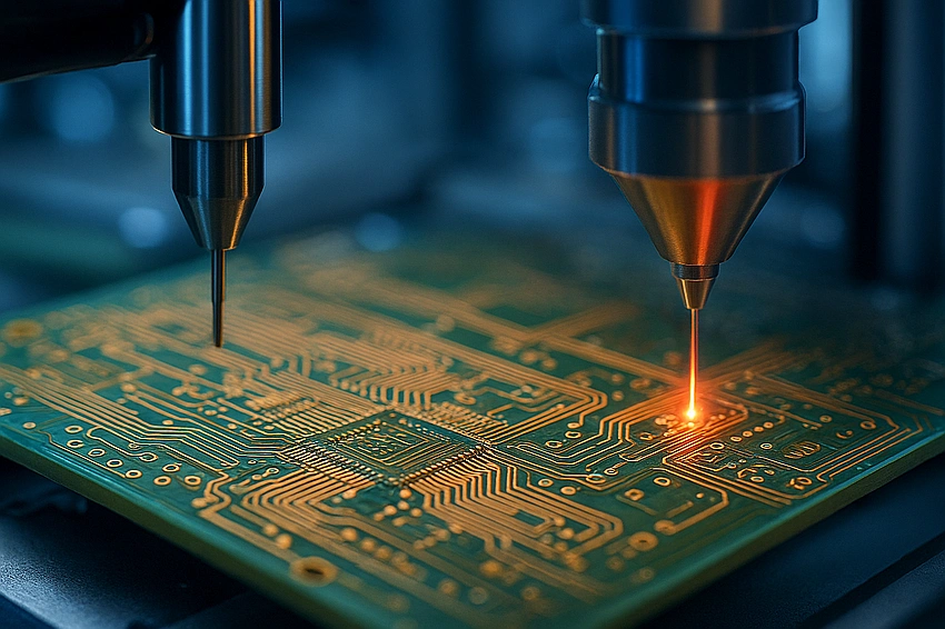
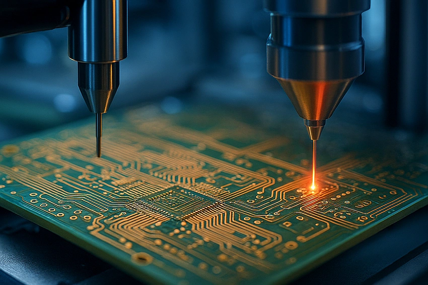
The manufacturing of HDI PCBs is more intricate than standard PCBs, often requiring sequential lamination and specialized equipment like laser drilling machines. A typical HDI board is built up in a layer-by-layer process, where layers are laminated, drilled, and plated multiple times. Common build-up structures are denoted as 1+N+1 or 2+N+2, where the numbers indicate the number of sequential lamination layers on the outside of the core (N), with higher numbers signifying greater complexity and density. Copper-filled microvias are also frequently used to enhance reliability and allow for stacked via structures, further maximizing routing efficiency.
Primary Advantages
The primary benefits of utilizing HDI technology are miniaturization and enhanced electrical performance. By consolidating multiple standard PCBs into a single, smaller HDI board, product size and weight are drastically reduced. Electrically, the shorter trace lengths and smaller vias in HDI designs result in improved signal integrity, lower signal loss, and reduced electromagnetic interference (EMI), which are crucial for high-speed digital and high-frequency applications. This enhanced performance and compact size also often lead to a lower overall system cost and faster time-to-market, despite the higher unit cost of the HDI board itself.
Common Applications
HDI PCBs are ubiquitous in contemporary electronics, finding their place in almost any device that prioritizes high performance in a small package. Their most common applications include consumer electronics like smartphones, tablets, laptops, and wearable devices. They are also vital in sophisticated systems across industries such as automotive electronics (e.g., ADAS, infotainment), medical devices (e.g., diagnostic equipment, implants), and aerospace and defense systems, where reliability and minimal size and weight are paramount.

Login to comment.
No thots yet. Be the first to share your thoughts!