PCB Manufacturing Processes Explained

PCB Manufacturing Processes Explained
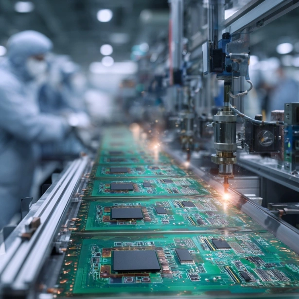
From the smartphone in your pocket to the complex avionics guiding an aircraft, Printed Circuit Boards (PCBs) are the foundation of virtually all modern electronics. They provide the mechanical structure and electrical connections for components, acting as the central nervous system of a device. While they may seem like simple green plastic boards, their creation is a precise, multi-stage process of chemical etching, lamination, and plating.
The journey from a digital design file to a physical PCB is a masterpiece of modern PCB manufacturing processes 🔗, requiring immense precision at every step. Here’s a look at the fundamental processes involved in bringing a circuit board to life.
Design and Pre-production
The entire process begins with a design, created using specialized EDA (Electronic Design Automation) software. The two main outputs are the Gerber files, which act as a blueprint detailing the copper traces, and the NC drill file, which specifies the location and size of all holes.
Before manufacturing begins, engineers perform a Design for Manufacturability (DFM) check. This crucial step ensures the design doesn't have any features—like traces that are too thin or holes that are too close together—that would cause problems or lead to a low yield during production.
Imaging, Etching, and Lamination
- Inner Layer Imaging & Etching: For multi-layer boards, the process starts with the inner layers. A sheet of laminate material, pre-covered with a layer of copper, is coated with a light-sensitive film called a photoresist. The Gerber file for an inner layer is used as a mask, and the board is exposed to UV light. The light hardens the photoresist over the desired copper traces. The board is then washed, and the unhardened resist is removed. Finally, a chemical solution etches away the exposed copper, leaving only the desired circuit pattern.
- Automated Optical Inspection (AOI): Once the inner layers are etched, they are scanned by an AOI machine. This high-resolution camera system compares the physical board to the original Gerber file, flagging any potential defects like shorts or open circuits. This is the last chance to fix errors on the inner layers.
- Lamination: The verified inner layers are stacked together with insulating layers of "prepreg" (fiberglass impregnated with resin) and copper foil for the outer layers. This "sandwich" is then placed in a high-temperature, high-pressure lamination press, which fuses the layers into a single, multi-layer board.
Drilling and Plating
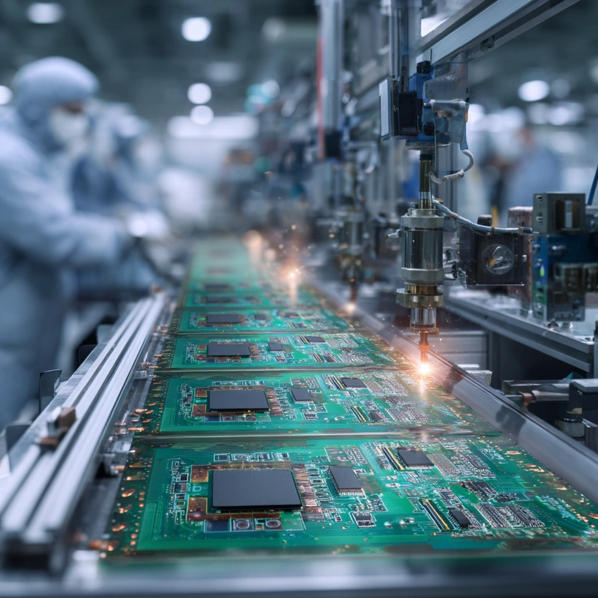
- Drilling: A computer-controlled drilling machine uses the NC drill file to precisely drill all the holes in the board. These holes, called vias, will connect the different layers of the circuit. For more advanced HDI (High-Density Interconnect) boards, high-power lasers are used to drill incredibly small "microvias."
- Copper Plating: The freshly drilled holes are non-conductive. To make them conductive, a very thin layer of copper is deposited chemically in a process called electroless plating. Following this, a thicker layer of copper is added through electrolytic plating (electroplating) to ensure a robust connection between the layers.
Outer Layers and Finishing Touches
- Outer Layer Imaging & Etching: The process used for the inner layers is repeated for the outer layers. A photoresist is applied, imaged with the outer layer patterns, and then etched, defining the final circuit on the board's surface.
- Solder Mask Application: To protect the copper traces from oxidation and to prevent solder bridges from forming between pads during component assembly, the board is covered with the iconic green (or other color) solder mask. Only the pads where components will be soldered are left exposed.
- Surface Finish: The exposed copper pads would quickly oxidize, making them difficult to solder. To prevent this, a protective metallic surface finish is applied. Common finishes include HASL (Hot Air Solder Leveling), ENIG (Electroless Nickel Immersion Gold), and OSP (Organic Solderability Preservative).
- Silkscreen: The final layer of ink, known as the silkscreen, is printed onto the board. This layer contains component designators, logos, and other markings that aid in assembly and identification.
Testing and Final Inspection
Before shipping, every board undergoes rigorous testing. An electrical test, often using a "flying probe" or "bed of nails" fixture, checks every connection for shorts and opens, ensuring the board matches the original design schematic perfectly.
Finally, the boards are cut from the larger manufacturing panel in a process called depaneling, and they undergo a final visual inspection before being packaged and sent to the customer for component assembly. This intricate dance of chemistry, mechanics, and optics is what makes the technology in our modern, connected world possible.
